
Surface analysis is the process of determining the structure and attributes of any arbitrary surface with resolution down to atomic/molecular layers (or even individual atoms/molecules).
Surfaces are frequently disordered at the atomic level in practice, therefore structural information must be understood in terms of some averaged and simplified model, which may not represent any specific structure on a real surface. Similarly, the sheer number of surface attributes of interest (biological, chemical, electrical, optical, magnetic, and so on) necessitates the employment of many techniques to thoroughly investigate the same surface.
Depending on the material, a surface layer can be up to three atomic layers thick (1 nm). Layers up to about 10 nm are called ultra-thin films, and layers up to about 1 m are termed thin films. The remainder of the solid is referred to as bulk material. Surfaces have an impact on a variety of variables, including corrosion rates, catalytic activity, adhesive qualities, wettability, contact potential, and failure mechanisms. Surface modification can be used to change or improve these features. Surface analysis techniques are thus critical for understanding a material’s surface chemistry and investigating the efficacy of surface engineering, material failures, or the development of new technologies.
The elemental composition and chemical state of materials that exist only in the surface number atomic layer can be analyzed with current surface analyzers, which is not achievable with other analysis methods.
Interesting Science Videos
Principle of surface analysis
To analyze a solid surface, it must first be activated in order to examine the signals that arise. For surface stimulation, light, x-rays, and electrons are utilized. Particles such as electrons and ions that are only given off by the surface are observed among the different signals that occur as a result of such surface stimulation, and their properties are analyzed to provide insight into the chemical structure of the surface.
The interpretation of a surface analysis experiment is often based on known (i.e., derived from theory or earlier observed from a standard sample) signatures of outgoing particles that are distinctive of a specific surface composition and/or structure. For example, lighting a surface with X-rays generates electrons (called photoelectrons), which have varied kinetic energies depending on the surface’s chemical composition. In another sort of experiment, escaping photoelectrons’ directions can be analyzed to produce an image of the surface or to gather information about the surface structure.
Why is surface analysis important?
- The composition of a material’s outermost atomic layers influences qualities such as chemical activity, adhesion, wettability, electrostatic charge, corrosion resistance, biocompatibility, and many more.
- Furthermore, pollutants, process residues, diffusion products, and impurities are commonly found near the surface of solid samples or at the interfaces of thin film structures.
- Sputter depth profiling offers a special chance to evaluate the materials employed in thin layers and to study how they interact with materials in neighboring layers by allowing thin film structures to be characterized.
- Analyzing sub-micron characteristics, defects, or particle pollutants is crucial to improving product yield in a wide range of materials systems and high-tech industrial products.
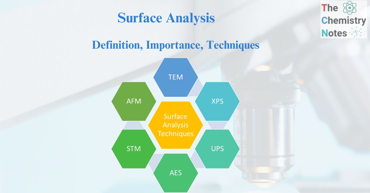
Types of surface analysis methods
The surface analysis process mainly involves three different methods. They are:
- Classical method
- Spectroscopic method
- Microscopic method
Classical methods of surface analysis
Classical methods of surface analysis provide useful information about the physical properties of surfaces but not so much about their chemical properties. They are usually applied for generating optical and electron microscopic pictures, as well as measurements of adsorption isotherms, surface areas, surface roughness, pore diameters, and reflectivity.
Spectroscopic methods of surface analysis
Spectroscopic methods of surface analysis give qualitative as well as quantitative chemical information about the composition of a few angstroms to hundreds of angstroms thick surface layers of a solid. There are various types of spectroscopic methods. Some of them are:
X-ray photoelectron spectroscopy (XPS)
The binding energy of photoelectrons that have been stimulated with a mono-energetic X-ray beam is measured by X-ray photoelectron spectroscopy (XPS) surface analysis tools to provide elemental and chemical state information.
The surface sensitivity and capacity to reveal chemical state information from the elements in the sample are two significant properties of this approach that make it powerful as an analytical tool. X-ray Photoelectron Spectroscopy (XPS), also known as Electron Spectroscopy for Chemical Analysis (ESCA), is a technique used to assess the quantitative atomic composition and chemistry of a substance.
Hard X-ray Photoelectron Spectroscopy (HAXPES)
It provides elemental and chemical state information, comparable to XPS, but from greater depths. This allows for the investigation of thicker film structures and deeper interfaces and also reduces surface contamination and ion-induced chemical degradation during depth profiling.
Ultraviolet photoelectron spectroscopy (UPS)
In UPS, photons irradiate a sample of interest and cause photoelectron ejection, similar to XPS; however, deep ultraviolet (UV) light is employed instead of X-rays. Because UV photons have lesser energy than X-rays, they expel valence band electrons rather than core-level electrons. Due to the reduced kinetic energy of UV photons, the photoelectrons measured are from the lower binding energy levels involved in bonding.
The utility of UPS is not in elemental analysis or oxidation state identification, as with XPS, but in measuring the valence shell electron ionization energies. This is especially crucial when attempting to determine the interaction of a chemisorbate with a surface or measuring the band structure of an inorganic or organic semiconductor.
SIMS ( Secondary Ion Mass Spectroscopy)
SIMS employs charged primary ions focused on a sample to sputter off atoms and molecules characteristic of the material’s outermost atomic layers. The principal ion dose can be carefully controlled such that surface damage is minimal, and the technology is non-destructive (so-called static SIMS). More ions per unit area can also be employed to sputter into the bulk of the material (this is known as dynamic SIMS). Chemical depth profiles can be obtained using this way of operation.
Time-of-flight secondary ion mass spectrometry (TOF-SIMS)
Surface analysis equipment using time-of-flight secondary ion mass spectrometry (TOF-SIMS) gives elemental, chemical, and molecular information by detecting the mass of ions ejected from a sample’s surface using a focussed ion beam. It has a very high surface sensitivity. It can extract organic compound molecular mass information and also can perform high-sensitivity inorganic element analysis.
Auger electron spectroscopy (AES)
AES ionizes electrons from the surface of a solid sample using a scanning focussed high energy electron source. An excited atom will then relax via an electron shell-to-shell transition, and the energy difference between the two shells must be released as either an X-ray or an outer shell electron emission – the so-called Auger electron.
AES is an electron spectroscopy technique that identifies electrons generated by Auger relaxation events. It is a semi-quantitative non-destructive core-level electron spectroscopy technique used to determine the elemental composition of surfaces, thin films, and interfaces.
Raman spectroscopy
It is a surface analysis technique that employs photons from a laser source, often in the infrared to ultraviolet wavelength range. Raman scattering occurs when a few incoming photons lose energy by stimulating vibrational modes in the material. A spectrum is created by detecting scattered photons. Raman spectroscopy often offers a considerably greater depth of investigation and is used to investigate molecular bonding in materials.
Raman spectroscopy is based on electromagnetic radiation’s inelastic scattering with the molecule. Raman spectroscopy can identify both inorganic and organic chemical groups. Many electron atoms, such as metals in coordination compounds, have a large number of loosely bound electrons and are thus Raman active. Raman can provide information on the metal-ligand bond, leading to knowledge about the complex’s composition, structure, and stability. This is especially beneficial in metal complexes with low IR vibrational absorption frequencies.
Temperature-programmed desorption (TPD)
There are several methods for researching surface reactions and molecule adsorption on surfaces that use temperature programming to distinguish between processes with varying activation values. The one that is most beneficial for single crystal research is temperature-programmed desorption.
Low-energy ion scattering spectroscopy (LEIS)
Low-energy ion scattering is an effective method for studying the “first monolayer.” LEIS, also known as ion scattering spectroscopy (ISS), is a low-energy form of Rutherford Backscattering Spectrometry (RBS). A LEIS study provides the atomic composition of the surface’s outer atomic layer, revealing the atoms that largely govern crucial activities like adhesion, catalysis, electron emission, and growth. Furthermore, LEIS provides non-destructive information about the in-depth distribution of elements within the near-surface region (0-10 nm), allowing analysis of ultrathin layers and interface diffusion.
It is a highly surface-sensitive surface analysis technique for probing the elemental composition of a surface’s first atomic layer. The probe employs a beam of noble gas ions scattered from the surface. The scattered ions’ kinetic energy is measured. As the incident beam’s energy, ion mass, scattering angle, and scattered ion energy are all known, conservation of momentum may be utilized to compute the mass of the surface atom.
Reflected electron energy loss spectroscopy) (REEL)
The spectrum distribution of energy transmitted from an incident electron beam into an object is measured using electron energy loss spectroscopy (EELS). The EELS spectrometer acquires the REEL spectrum using a reflected electron beam. Multiple valence losses occur in more than half of the reflected electrons. The REEL spectrum shows the intensity distribution of reflected electrons as a function of energy loss and is very sensitive to surface electrical structure.
It operates similarly to ISS, except that the incoming particle is an electron, and the scattered electron beam is monitored. The incident electrons can lose energy by generating electronic transitions in the sample, and the REELS experiment measures these energy losses. It is possible to measure properties such as electronic band gaps or the relative energy levels of vacant molecular orbitals.
Microscopic techniques of surface analysis
Microscopic methods of surface analysis provide useful information about the elemental and chemical composition of the materials. Different microscopic techniques involve:
Scanning electron microscopy (SEM)
The electron beam scans the material in a raster pattern in SEM. Electrons are reflected on the surface instead of going through the specimen, and they can even ionize atoms within the sample by freeing electrons. Secondary electrons, as well as backscattered electrons, can be used as signals to construct the final image. SEM pictures represent a sample’s morphology and can reconstruct quasi-three-dimensional views of the sample surface. As a result, the technique is primarily utilized to generate a high-resolution image of surface features and to draw inferences regarding the distribution of various chemical elements within the sample.
So, In SEM An electron beam is created by a high-voltage electron gun and focussed onto the surface of the sample using electromagnetic lenses in an SEM. Electrons interact with the atoms in the sample, producing secondary electrons and other types of electromagnetic radiation, such as X-rays, to be emitted. Detectors detect the released particles, and the data is used to build a high-resolution image of the sample’s surface.
SEM is used in various domains of biological study, including cell and molecular biology to investigate cell morphology, microbiology to investigate bacteria and viruses and their interactions with surfaces, each other, and other cells, and genetics to investigate gene expression. Additionally, in materials science, scanning electron microscopes (SEMs) are used for research, quality control, and failure analysis.
Scanning tunneling microscopy (STM)
STMs have been used in nano-machining and the formation of nano-features through using localized heating or the stimulation of chemical processes immediately under the STM tip.
The scanning tunneling microscope (STM) scans a surface with a sharp metal wire tip. High-resolution images of the surface, down to the level of individual atoms can be obtained by positioning the tip very close to the surface and applying a voltage to the tip or sample.
Atomic Force Microscopy (AFM)
The AFM works on the cantilever principle; a small hook is attached to one end of the cantilever, and the force applied by the tip on the sample is measured by monitoring the deflection of the cantilever. In this technology, light is reflected off the surface of the cantilever and into a position-sensitive detector. As a result, even a tiny bend in the cantilever will produce a tilt in the reflected light, moving the position of the beam such that it falls at a different angle on the detector.
Atomic Force Microscopy (AFM) is a high-resolution imaging technique that can resolve features as small as an atomic lattice. It is also known as a scanning probe microscope (SPM). The atomic force microscope (AFM) is being used to solve processing and material challenges in a wide range of technologies that are influencing a wide range of industries, including the energy, automobile, aerospace, biological, and telecommunications industries. Nearly every material, from polymers and ceramics to composites and composite materials, can be investigated using AFM.
Transmission electron microscopy (TEM )
Transmission electron microscopy (T EM) is a microscopy technique in which an electron beam is transmitted through an ultra-thin object, interacting with it as it passes. The interaction of electrons passing through the specimen produces an image, which is magnified and focussed onto an imaging device, such as a fluorescent screen, a layer of photographic film, or a sensor, such as a CCD camera.
TEM devices provide information on the topography, morphology, atomic composition, and crystal structures of materials. It provides the highest magnification of any magnifying technique. The images produced by TEM surveys are of excellent resolution and provide information about the molecular structure, shape, size, and nanosurface characteristics of the materials.
TEM is used in the development of products as well as the manufacturing processes of advanced manufacturing industries such as semiconductors and nanotechnology. TEM instruments are used in various research areas including virology, materials science, nanotechnology, semiconductor research, environmental sciences, and even paleontology and palynology use TEM instruments.
References
- https://www.britannica.com/science/surface-analysis.
- https://assets.thermofisher.com/TFS-Assets/MSD/Reference-Materials/WP0016-scanning-electron-microscopy-working-principle.pdf.
- https://www.lpdlabservices.co.uk/analytical_techniques/surface_analysis/index.php.
- https://www.eag.com/services/materials/surface-analysis/.
- https://biointerface.org/surface/.
- https://chem.libretexts.org/Bookshelves/Physical_and_Theoretical_Chemistry_Textbook_Maps/Surface_Science_(Nix)/05%3A_Surface_Analytical_Techniques.
- https://www.nrel.gov/docs/gen/fy04/36831n.pdf.
- https://web.iyte.edu.tr/~serifeyalcin/lectures/chem502/L5.pdf.
- https://www.ulvac-phi.com/en/surface-analysis/analysis/#:~:text=The%20characteristics%20and%20features%20of,layer%20of%20the%20solid%20matter.