
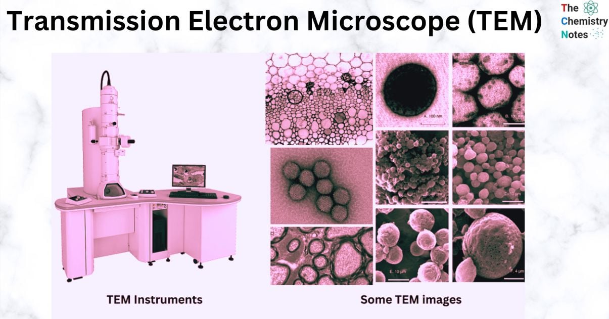
Transmission electron microscope offers information about the microscopic structure, crystal structure, and micro-chemical from each of the microscopic phases individually and with high spatial precision. It generates a magnified image by focusing an electron beam on a sample. Objects can be magnified up to a million times with a TEM. Therefore, TEM is a highly effective method for characterizing materials. TEM research is useful not only for a better understanding of structure-property relationships but also for the development of high-performance alloys.
By using a beam of electrons to produce wave motion, Louis de Broglie’s early discovery of cathode rays like electrons in the early 1920s cleared the path for the construction of an electron microscope. To focus the electrons, magnetic fields were employed. Based on these findings, Ernst Ruska and Max Knolls created the first electron microscope in 1931, then in 1933, Ernst Ruska collaborated with the Sieman’s firm to create the transmission electron microscope (TEM).
What is a Transmission Electron microscope?
An analytical method for visualizing microscopic structures is transmission electron microscopy (TEM). TEM can magnify nanometer-size objects up to 50 million times, revealing astonishing detail at the atomic scale in contrast to optical microscopes, which only use light in the visible spectrum. Because electrons, when accelerated in a strong electromagnetic field, can have a wavelength around 100,000 times smaller than that of visible light, the resolution of a microscope can be improved by many orders of magnitude.
Thin “electron transparent” samples, typically thinner than 100 nm, are used to create Transmission electron microscope images by accelerating a high-intensity electron beam through them. Focusing the beam on the sample, reducing distortions, and magnifying the resulting picture onto a phosphor screen or specialized camera are all accomplished using a set of electromagnetic lenses and apertures distributed throughout the microscope’s column.
Why transmission electron microscopy is used?
Comparatively, scanning electron microscopy can only reveal a specimen’s morphology, while this method can reveal its structure, crystallization, morphology, and stress. However, specimen preparation can be more time-consuming for TEM because it requires very thin, semi-transparent electron samples.
Principle of Transmission Electron Microscope
The transmission electron microscope (TEM) operates using a principle that is very similar to that of the light microscope. The most important distinction is that light microscopes use light rays to concentrate and generate an image, whereas transmission electron microscopy (TEM) utilizes a beam of electrons to focus on the object and produce an image.
When compared to light, which has a very large wavelength, electrons have a relatively small wavelength. The process behind a light microscope is that an increase in resolution power results in a shorter wavelength of light. On the other hand, the mechanism behind a transmission electron microscope (TEM) is that when the specimen is illuminated by the electron, the resolution power increases, resulting in a longer wavelength of the electron transmission. Since the wavelength of an electron is around 0.005 nm, which is 100,000 times shorter than the wavelength of light, the transmission electron microscope (TEM) has approximately 1000 times higher resolution than a light microscope. It has been demonstrated that the transmission electron microscope (TEM) can be utilized to provide a comprehensive illustration of the interior structures of even the smallest particles, such as a virion particle.
The conventional transmission electron microscope has two modes of operation:
- Image mode: Transmission electron microscopy is used to obtain a high-resolution image of a thin sample by passing the electron beam through the sample and projecting the electrons onto a camera. Traditional TEM makes use of three different picture modes: bright field, dark field, and high-resolution electron microscopy, also called a phase-contrast mode.
- Diffraction mode: In diffraction mode, the electron beam obtained from the sample is used to illuminate a diffraction pattern on a fluorescent screen. The diffraction pattern is identical to that produced by x-rays. A single crystal will show as a succession of spot on the screen, while a polycrystal will show as a series of powdery rings or hazy halos.
Instrumentation of Transmission electron microscope
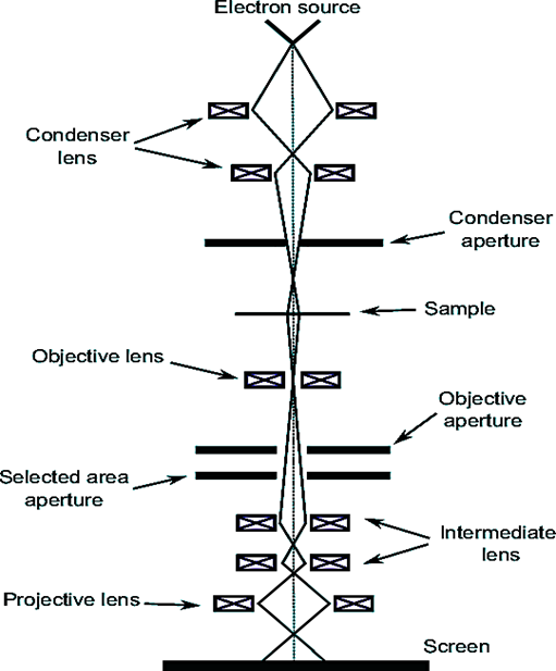
- Electron source: The electrons used in illumination come from a gun that uses either thermionic or field emission technology.
- Condenser lens: To focus the beam, the first condenser (Electromagnetic type) lens uses an aperture or slit to restrict the entry of wide-angle electrons. The beam is concentrated on a small area of the sample by the second condenser lens.
- Objective lens: The objective lens gathers the electrons that pass through a thin sample. The objective lens’s rear aperture is where the appropriate operating mode is chosen.
- Projective lens: The objective lens creates a focused image, which is then enlarged by an intermediate lens and a projection lens.
- Detector: To capture an image of the sample, the magnified image is projected onto an electron-sensitive camera.
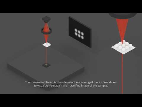
How Does Transmission electron microscope Work?
A TEM’s functioning is comparable to that of a slide projector. Light from a projector is sent through the slide, and the structures and objects on the slide modify the light as it travels through. This causes the light beam to be partially blocked from passing through the slide. An expanded version of the slide is formed when the transmitted beam is projected onto a screen. Here is a more in-depth description of how a standard Transmission Electron Microscope operates:
- The electron gun at the top of the microscope produces a stream of monochromatic electrons.
- By using condenser lenses 1 and 2, this flow is focused into a narrow, coherent beam. The size of the spot, where the electron beam hits the sample, is set by the first lens. The second lens condenses the light to a pinpoint on the sample, transforming it from a broad, diffused spot.
- The Condenser aperture narrows the beam, blocking electrons at high angles of incidence (those away from the optic axis, the dotted line along the center).
- A part of the beam that strikes the specimen is transmitted.
- This transmitted portion is focussed by the objective lens into an image.
- Optional goal and area of focus Metal apertures have the ability to confine the beam, with the objective aperture boosting contrast by excluding high-angle diffracted electrons and the selected area aperture allowing users to analyze the periodic diffraction of electrons by organized arrangements of atoms in the sample.
- Through the intermediate and projector lenses, an image is gradually magnified as it travels down the column.
- The operator sees the image because light is produced when the beams strike the phosphor image screen. Areas with low electron transmission appear darker (thicker or denser) because of this. More electrons were able to pass through the thinner or less dense parts of the sample, which are depicted by the brighter parts of the image.
The electron beam’s interaction with electrons in the specimen creates a wide range of radiation that can be used to learn a great deal about the sample. No energy disappears during the production of diffraction patterns by elastic scattering. The intensity of the transmitted electrons might vary due to the inelastic interaction between the electron beam and the electrons at dislocations, grain boundaries, and second-phase particles in the sample. Scattering in both the elastic and inelastic regimes can provide extensive details about the sample. TEM instrument lateral spatial resolution increases with operating voltage. 400 kV TEM instruments have point-to-point resolutions better than 0.2 nm. Because high-energy electrons interact less strongly with matter than low-energy electrons, high-voltage TEM equipment has greater electron penetration. High-voltage TEMs can handle thicker samples. TEM has low depth resolution. TEM images show electron scattering from a three-dimensional sample on a two-dimensional detector.
Transmission Electron Microscope Sample Preparation and Visualization
It is challenging to prepare samples thin enough to be electron-transparent, but nanomaterials make this process much simpler. Solid components absorb and scatter electrons, making thick specimens difficult to visualize. Thus, thin specimens are used for accurate viewing and sharp images. The specimen should be 20-100 nm thin and 0.025-0.1nm wide, like a bacterial cell. Thin specimens interact with electrons in a vacuum and maintain their structure. Fixing the specimen on plastic with glutaraldehyde or osmium tetra-oxide yields thin-slice specimens. These chemicals maintain cell structure and uniqueness. Ethanol will dry the cell for plastic embedding. An unpolymerized liquid epoxy plastic permeates the specimen, hardening it into a block. This is where ultramicrotomes cut thin slices with glass knives. The specimen is dyed to uniformly scatter electrons. The thin sections are bathed with lead citrate and uranyl acetate to bind lean and aluminum ions to cell structures. This opaquely shields cell structures from electrons. To facilitate viewing, the stained thin pieces are placed on copper grids. For examination in the TEM, negative staining, often in combination with a coating of heavy metallic components, is the preferred method of staining. Uncoated sections are utilized to examine bacterial and viral cell morphologies and structures, while the metallic coating scatters electrons that appear on photographic film.
When it comes to determining the crystal structure of nanomaterials like nanocrystals and nanorods, as well as the crystal structure of distinct regions of a sample, selected area diffraction (SAD) is in a league of its own. Defocusing the condenser lens to create parallel illumination at the specimen and using a predetermined area aperture to restrict the diffracting volume constitutes SAD. Similar to the way XRD is utilized, SAD patterns are analyzed to identify the Bravais lattices and lattice parameters of crystalline materials. However, electron scattering is extremely sensitive to the target element, and several spectroscopy techniques have been developed for the investigation of chemical composition, thus TEM is still useful for a wide range of chemical analyses.
Nanocrystal melting points have also been calculated using TEM. The loss of crystalline diffraction is an indication that an electron beam has heated a nanocrystal to the point of melting. Mechanical and electrical properties of individual nanowires and nanotubes have also been measured using TEM. Because of this, structure-property correlations in nanomaterials can be established.
HRTEM is best for imaging atomic-scale defects. It depicts a two-dimensional crystal with flaws and other properties in good examples. This only makes sense if the two-dimensional projection is down a low-index direction and atoms are perfectly on top of each other. Consider a very thin slice of crystal slanted so that a low-index direction is exactly perpendicular to the electron beam. All lattice planes parallel to the electron beam will refract the primary beam since they are near the Bragg position. Crystal diffraction patterns are Fourier transforms of the periodic electron potential. The objective lens reunites the diffracted beams and the source beam to back transform and expand the periodic potential.
Advanced Techniques of Transmission electron microscope
Developments in electronics, electron optics, and lens fabrication have led to tremendous improvements since the first prototype TEM, which had an image magnification of 17 times. These developments have led to the current dedicated high-resolution TEM, which is capable of sub-Angstrom spatial resolution and has the potential to record images with a magnification of over a million times. Resolutions of less than 0.1 nm have been attained by utilizing field emission gun electron sources in conjunction with aberration corrected lenses. In addition, computational capabilities have advanced to the point that it is now possible to anticipate the properties of materials using computer models that include a similar number of atoms. This may be shown by using high resolution transmission electron microscopy (HRTEM).
The rapid development of new materials for strategic applications, as well as the equally rapid expansion of nanotechnology and semiconductor technology, necessitate ever-improving transmission electron microscopes. Crystal structure of the various phases can also be acquired by using chosen area and microdiffraction techniques in TEM, in addition to lattice imaging by HRTEM for studying interfaces, defects, and precipitation studies. Information on the crystal’s symmetry, lattice, stresses, thickness, etc. can be extracted from small, precisely located samples using convergent beam electron diffraction (CBED). CBED offers an advantage over X-ray diffraction in that it allows for the simultaneous acquisition of symmetry information, morphology, interface coherency/defect structure, and micro-chemistry from localized sub-microscopic regions.
Energy dispersive analysis of X-rays (EDAX) and electron energy loss spectroscopy (EELS) can provide insight into the micro-chemical composition of a material. EELS has the ability to detect and identify elements down to a relatively low atomic number because to its high sensitivity and spatial resolution. In addition to elemental concentrations, EELS allows for the spatially resolved determination of electron density, density of states, electronic structure, site symmetry, radial distribution functions, and specimen thickness.
In addition to analytical methods like EDAX and EELS, a technique dubbed ALCHEMI (Atom Location by CHanelling Enhanced MIcroanalysis) based on the electron channelling effect can be utilized to locate specific element sites of occupation in ordered crystals. In fact, modern technology has progressed to the point where the microscope may be operated from a control room far from the actual microscope by means of a computer equipped with a web browser and the appropriate interface. TEM is an indispensable tool in the development and characterization of advanced materials due to its ability to provide information on a material’s microstructure, crystal structure, symmetry, lattice strain, interface lattice structure, micro-chemistry, bonding state of constituent elements in the phase, etc. Examining flaws in crystals is a popular application of TEM technology.
Electron beams, in contrast to X-rays, may be focused with the use of magnetic fields and are therefore capable of being employed for imaging. Magnetic fields can function as convex lenses, focusing electron waves as they pass through them. Even with magnetic lenses, lens aberrations are notoriously difficult to rectify, just as they are with traditional optical lenses. However, the intensity distribution of the electron waves as they leave the material is able to be enlarged by an electron optical system, which makes it feasible to achieve resolutions of less than 0.1 nm.
Electrons can interact with the material in two different ways: either through inelastic scattering or elastic scattering. In order to produce adequate picture contrast, inelastic scattering, which eventually leads to absorption, must be avoided. This is because inelastic scattering does not include any local information. After that, the electron beam will become elastic. The amplitude and phase of the incident and diffracted beams are both modulated as a result of the lattice imperfections.
In transmission electron microscopy (TEM), a specimen that is less than 200 nanometers thick is passed through an electron beam that has an energy of 100 keV or more (up to 3 MeV). Transmission electron microscopy (TEM) has an exceptional resolution that can reach down to one Angstrom, high magnifications that can reach up to 106, and it can function as both a microscope and a diffractometer. The reduction of inelastic electron scattering is of the utmost importance; as a result, the thickness of the specimen must be between 10 nanometers and one micrometer. The resolution is proportional to the thickness, therefore high-resolution transmission electron microscopy (HRTEM) requires specimen thicknesses in the nanometer range.
Quantitative analysis using Transmission electron microscope
TEM investigations provide practically all of the granular information that is available regarding prolonged defects. These investigations not only display the defects, but also, via the application of appropriate theory, provide quantitative information regarding, for example, strain fields. Not only does the electron-optical system help to magnify the intensity (and, in HRTEM, the phase) distribution of the electron waves exiting the object, but it also provides electron diffraction patterns with the flip of a switch.
It is feasible to satisfy the Bragg requirement either for several, only two, or none of the reciprocal lattice vectors by angling the specimen about the incident electron beam. This can be accomplished by tilting the specimen. The ‘two-beam’ situation in which only one ‘reflex’ is activated is the preferred condition for regular imaging. This means that the Bragg condition is only satisfied for one point in the reciprocal lattice or one diffraction vector g [often with tiny Miller indices, such as 111 or 220]. The preparation of the specimen is always the most difficult part of TEM research. It is a difficult challenge to obtain specimens that are thin enough and include the faults that need to be evaluated in the appropriate geometry (for example, in cross-section). The following information can be obtained with a transmission electron microscope (TEM), which is modeled after the transmission light microscope.
Moreover, it gives quantitative information in terms of:
- Morphology: How the particles that make up the specimen compare to one another in terms of size and shape at the subatomic level.
- Crystallographic information: The arrangement of atoms in the specimen and their degree of
- order, detection of atomic-scale defects in areas a few nanometres in diameter.
- Compositional information: Composition and abundance of individual elements and compounds down to the nanometer scale.
Application of Transmission Electron Microscope
- Crystallographic, compositional, morphological, and topographic information can all be obtained from TEM images.
- The images provide a molecular-level perspective, letting scientists examine sample structure and texture in incredible clarity. Industrial applications aside, this information is helpful in the study of crystals and metals.
- Tech businesses rely on TEMs to inspect tiny objects for damage and defects so that they can improve the product’s quality and longevity.
- TEMs have applications in the analysis and production of semiconductors, as well as in the production of computer and silicon chip components.
- It will provide individuals a chance to see the microscopic Worlds of nanotechnology closely and personally.
Advantages of Transmission Electron Microscope
- Magnification can be increased by a factor of a million or more with a transmission electron microscope (TEM).
- The many scientific, educational, and industrial disciplines that can benefit from using TEMs are remarkable.
- High-angle annular dark field (STEM) and dark/bright field (TEM) imaging, as well as phase contrast (TEM).
- It allows us to gain insight into the cells of microorganisms including bacteria, viruses, and fungi.
- TEMs can provide details about a sample’s size, shape, and structure simply by examining its surface.
- TEMs reveal the composition of individual elements and compounds.
- High-resolution, detailed images
- With the right instruction, they can be operated with ease.
- Damaged microparticles can be repaired after being detected and identified using this method.
Limitations of Transmission Electron Microscope
- It’s a rather costly method of imaging.
- All samples must be electron transparent, vacuum chamber safe, and small enough to fit inside the chamber.
- Getting specimens ready to be observed by TEM is a time-consuming process.
- Artifacts can be dangerous due to the usage of chemical fixations, dehydrators, and embedders.
- Specialized housing and maintenance are necessary for TEMs.
- Due to their sensitivity to electromagnetic and vibrational fields, they are typically deployed in secure locations.
- The visuals it creates are monochromatic unless a fluorescent screen is added at the end of the visualization process.
Watch out for the animated video to learn the working principle of Transmission Electron Microscope
References
- D. B. Williams and C. B. Carter, Transmission Electron Microscopy, Springer, 2009.
- C. R. Brundle, C. K. Evans, Jr., S. Wilson and L. E. Fitzpatrick (eds), Encyclopedia of Materials Characterization: Surfaces, Interfaces, Thin Films, Butxetworch-Heinemann, Reed Publishing (USA) Inc., 1992.
- https://chemistnotes.com/physical/transmission-electron-microscopy-principle-instrumentation-and-application/
- Katerina Mrazova, Jaromir Bacovsky, Zuzana Sedrlova, Eva Slaninova, Stanislav Obruca, Ines Fritz, Vladislav Krzyzanek, Urany-Less Low Voltage Transmission Electron Microscopy: A Powerful Tool for Ultrastructural Studying of Cyanobacterial Cells, Microorganisms, 10.3390/microorganisms11040888, 11, 4, (888), (2023).
- https://microbenotes.com/transmission-electron-microscope-tem/