
The scanning tunneling microscope (STM) developed by Dr. Gerd Binnig and his colleagues in 1981 at the IBM Zurich Research Laboratory, Ruschlikon, Switzerland, is the first instrument capable of directly obtaining three-dimensional (3D) images of solid surfaces with atomic resolution. STMs have been put to use in the nano-machining process, as well as the development of nano-features by the application of localized heating or the induction of chemical reactions directly under the STM tip. Nanofabrication and nano machining are two applications that have made use of AFMs.

STMs and AFMs are utilized for imaging macro to atomic dimensions with high-resolution information and for spectroscopy at extreme magnifications ranging from 103 to 109 in the x-, y-, and z-directions, respectively. These instruments are versatile enough to be utilized in any environment, including ambient air, a variety of gases and liquids, a vacuum, and temperatures as low as approximately 100 K or as high as about a million degrees Celsius.
Electron Tunneling
Giaever was the one who first postulated the principle of electron tunneling. He theorized that because electrons have the ability to travel through potential barriers, a current would flow between two metals that were separated by a thin insulating membrane if a potential difference was applied to the system.
- Even if it’s not very likely, there is still a possibility of tunneling. It is necessary that the distance between the two metals be no greater than 10 nanometers in order to accurately quantify a tunneling current.
- The tunneling current is extremely sensitive to the distance that separates the tip from the sample; it drops at an exponential rate as the tip–sample separation distance increases.
- This component is essential to ensure that the scanning tunneling microscope (STM) maintains its exceptional vertical resolution (less than 0.1 nm).
- The tunneling current drops by a factor of two whenever the distance between the two points is increased by 0.2 nanometers. Extremely high lateral resolution is dependent on having sharp tips.
- Both the damping of external vibrations and the movement of the tunneling probe into close contact with the sample were challenges that Binnig and his team were able to overcome.
- Their apparatus is known as a scanning tunneling microscope, or STM for short. STMs of today can take images of surfaces at atomic size even when employed in their natural environments.
Principle of STM
- The STM operates on a simple and well understood basis. A sharp metal tip, which serves as one electrode of the tunnel junction, is brought close enough (0.3–1 nm) to the surface that is the focus of the investigation, which serves as the second electrode.
- This proximity ensures that the tunneling current, which can be measured, varies from 0.2 to 10 nA when the working voltage is between 10 mV and 1 V. Tunneling current between the tip and the surface is measured as the tip is scanned across the surface at a distance of 0.3–1 nm.
- In scanning tunneling microscopy (STM), a conductive tip is moved along the surface of a sample while its height is continuously modified to maintain a constant tunneling current. The tip is held above the surface of the sample. In order to map the topography of the sample’s surface, the position of the tip is tracked. A simplified representation of an STM structure. On a stage that accommodates three-dimensional positioning is a pointed tip made of tungsten or PtIr alloy.
- Piezoelectric arrays are responsible for controlling the movement of the tip in three dimensions relative to the sample surface.
- The distance between the tip and the sample is around 0.2 to 0.6 nm, which results in a tunnelling current that ranges from approximately 0.1 to 1.0 nA.
- This results in a genuine atomic resolution across all three dimensions, with a spatial resolution of approximately 0.01 nm in the x- and y-directions and approximately 0.002 nm in the z-direction.
How does STM work?
A sharp metal wire tip is scanned over a surface in the scanning tunneling microscope (STM). By placing the tip very close to the surface and applying a voltage to the tip or sample, we can produce incredibly high-resolution images of the surface, down to the level of individual atoms.
Several principles serve as the foundation for the STM. As discussed below, a 3D image of the electronic topography can be generated by tunneling from the tip to the surface, rastering the tip using piezoelectric positioning, and keeping a constant current point in a feedback loop.
Tunneling: When electrons pass through a barrier they shouldn’t, a tunneling current ensues. If you don’t have the energy to “over” a barrier, you won’t. Electrons are wavelike in quantum mechanics. At a wall or barrier, these waves quickly fade. If the barrier is thin enough, the probability function may pass through it! Given enough electrons, some will cross the barrier due to the low probability of an electron being on the other side.
Tunneling occurs when an electron passes past the barrier. To apply this concept to the STM, we may say that, depending on how the device is set up, the electron beam originates from the tip or the sample. The first region is the air, vacuum, or liquid separating the tip from the sample, while the second is the other side of the experiment. We can precisely regulate the tip-sample distance by monitoring the gap current.
Piezoelectric Effect: Scanning tunneling microscopy (STM) and other scanning probe techniques rely on these components to scan the tip. Scanning probe microscopy frequently employs PZT (lead zirconium titanate), a piezoelectric material.
Feedback loop: Electronics are required for STM imaging because they monitor the current, scan the tip, and convert the data into a form usable by the microscope. A feedback loop continuously measures the tunneling current and makes necessary modifications to the tip.
The computer records these alterations and displays them as an image within the STM program. A steady current image describes this type of arrangement. Additionally, the feedback loop can be disabled, leaving only the current reading, for extremely flat surfaces. This image has the same height throughout.
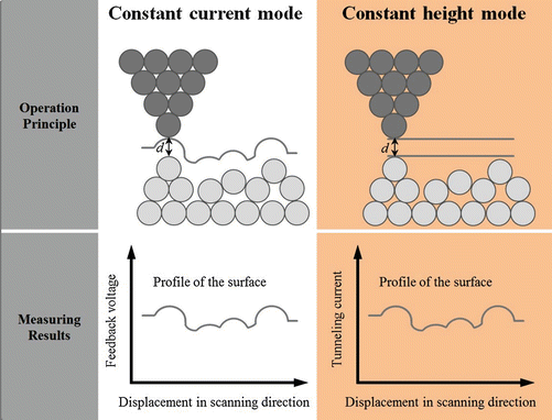
Modes of operation
The STM can often be operated in one of two modes.
- One of these techniques is called continuous current imaging, and it involves keeping a constant current flowing between the sample and the tip of the instrument. Changing the tip’s vertical position as it moves over the surface of the sample helps ensure that there is a uniform amount of space between the sample and the tip throughout the whole process. Imaging with a constant current will provide excellent surface topographic contrast of the surface atom contours because the tunnelling current is sensitive to distance.
- In contrast to the constant current mode, the constant tip position mode results in fluctuations in the tunnelling current due to changes in tip separation distance brought about by the three-dimensional topographic characteristics of the surface atoms. These variations in tunnelling current are caused by the fact that the constant tip position mode is used.
- When operating in the constant current mode, the contrast is determined by the electron charge density profiles; however, when operating in the constant height mode, faster scan rates are possible.
- The STM can work in either a constant height mode or a constant current mode, with the mode that it uses being determined by a parameter setting made in the control panel. In the constant current mode, the feedback gains are turned up high, the tunneling tip follows the sample surface very closely, and the change in tip height that is required to maintain constant tunnelling current is monitored by the change in the voltage that is delivered to the piezo tube. In the variable current mode, the feedback gains are not changed.
- When operating in the constant height mode, the feedback gains are reduced, the tip of the instrument maintains a height that is nearly constant as it travels over the sample surface, and an image of the tunneling current is produced.
Instrumentation of STM
The instrumentation of STM is depicted below:
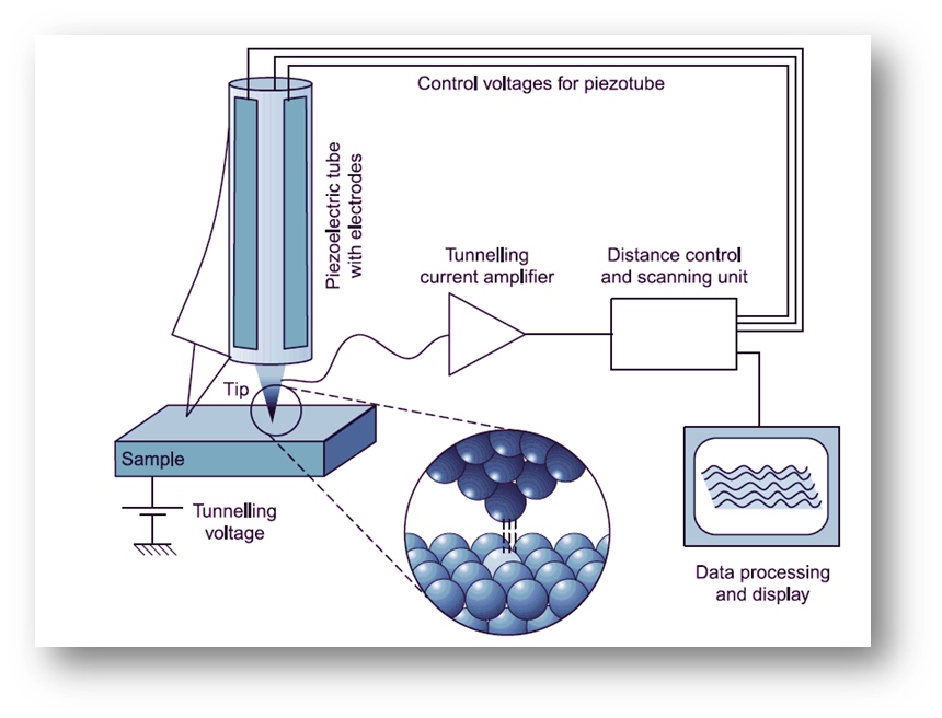
- Probe tip: Since it is the probe tip that makes contact with the specimen, it is an essential component of the STM. The probe’s tip is the most important part since it affects how sharp the final image will be. Typically, metals like tungsten or platinum-iridium are used for STM probes.
- Piezoelectric tube: Typically, piezoelectric transducers are used to regulate the tip’s position in all three dimensions. For x and y motion in an STM arrangement, a computer communicates directly with piezo crystals. Measurements of constant tunneling current can also include a feedback loop to regulate the Z motion (which controls the probe height).
- Electronics: Simple, yet highly sensitive and accurate circuits are used in an STM. The specimen is first subjected to a low voltage from a voltage source. A tiny tunneling current, on the order of 10-9 A, is produced when the probe is at a typical scanning distance (1 nm, or 10-9 m). This low-level current is amplified by an electronic device and then used to trigger other electronic devices.
- Environmental Chamber: In contrast to electron microscopy, the physics of the STM technique does not necessitate any unusual circumstances. However, STM requires a highly controlled environment to keep surfaces clean, as it is sensitive to contamination.
- Vibrational Isolation: Since STM measures distances on the order of 0.1 nm or less, it is especially vulnerable to vibrations compared to other types of microscopy. The operation of an STM can be substantially limited or even prevented by even subtle vibrations from a nearby road or other lab equipment. That’s why the STM relies entirely on stiff construction. Also, the STM apparatus needs to be mounted on air springs or other vibration-isolating hardware to prevent unwanted movement. For this reason, STM location inside a structure is equally crucial.
Components of STM
The STM is composed of three basic components;
- Head: It has a pre-amplifier circuit (FET input amplifier) mounted on the top of the head for the tunneling current and a piezoelectric tube scanner for the tip’s three-dimensional motion.
- The base that the sample is mounted on, as well as the base support that holds both the base and the head in place. The base can accommodate samples with dimensions up to 10 millimeters by 20 millimeters and with a thickness of 10 millimeters.
- The STM has a range of scan sizes available, including 0.7 micrometers (for atomic resolution), 12 micrometers, 75 micrometers, and 125 micrometers square. The scanning head is responsible for controlling the movement of the tip in all three dimensions. Because of the excellent thermal compatibility between the piezotube and the invar, the detachable head consists of a piezo tube scanner that is approximately 12.7 millimeters in diameter and is mounted inside of an invar shell. This configuration helps to minimize vertical thermal drifts.
- The x, y, and z movements of the piezo tube are each controlled by their electrodes, which are in turn driven by their driving circuits.
- The design of the electrodes gives x- and y-motions that are perpendicular to each other, reduces horizontal and vertical coupling as much as possible, and has a high degree of sensitivity. The Z electrode, which is powered by the feedback loop, regulates the vertical motion of the tube so that it may be precisely regulated.
- Both the x-scanning motion and the y-scanning motion are each controlled by their own set of two electrodes. These electrodes are powered by voltages that are the same magnitude but have opposing signs. These electrodes are referred to as Y, X, +Y, and +X, respectively.
- The tip holder is a stainless steel tube that has a 300 micron inner diameter and can accommodate tips with a 250 micron diameter.
- The tube is mounted in ceramic so that the bulk at the end of the tube is kept to a minimum.
- The tip can be fixed either on the front edge of the tube (to maintain a low mounting mass and a high resonance frequency) or in the middle of the tube (to maintain the symmetry of the scanning) for large range scanners such as 75 m and 125 m.
- Any tip with a shaft diameter of 250 micrometers or less can be used with this commercial STM. The piezo tube needs to have its X and Y coordinates calibrated, which can be accomplished by photographing an acceptable calibration standard. For longer range heads, two-dimensional grids, which include a gold-plated ruling, can be employed in place of cleaved graphite. Cleaved graphite is utilized for shorter scan length heads.
Difference between Atomic Force Microscopy (AFM) and Scanning Tunneling Microscopy (STM)
The employment of AFMs and STMs is common in nano-science. However, they each have their own set of benefits and drawbacks when it comes to measuring particular properties of samples, as dictated by their underlying working principles. In order for the tunneling current to flow through the tip and the sample, an electric circuit must be created.
- For STM, this means the sample needs to have good conductivity. However, in the case of AFM, the deflection of the cantilever due to van der Waals forces between the tip and sample is all that is measured. As a result, AFM can be applied to virtually any sample.
- STM, however, has more resolution than AFM due to the exponential relationship between tunneling current and distance.
- AFM images are highly dependent on the tip’s shape and contact force, while STM images make it possible to “see” individual atoms.
Sometimes it can be difficult to extrapolate from the observed signal to conclusions about the sample’s morphology or other features. However, STM can provide a more direct electric property of the sample’s surface.
Advantages of STM
Because STMs provide a three-dimensional profile of a surface, scientists can investigate its roughness, surface defects, and other properties, as well as learn more about the molecules themselves, including their size and conformation. Besides these, some of the major advantages of STM are:
- Superior to less powerful microscopes in their ability to capture fine-detail images. As a result, scientists have a better molecular understanding of their study’s topic.
- Versatility: They function in a wide variety of environments, including a vacuum, air, water, and other liquids and gases.
- From absolute zero Kelvin to several hundred degrees Celsius, they may function normally.
Limitations of STM
- It might be challenging to get the most out of an STM. It is a highly complex method that requires exceptional expertise and care. Stable and clean surfaces, low vibration, and a pointed tip are all necessary for STMs.
- STMs rely on expensive, delicate, and specialized machinery.
Applications of STM
From biology and materials science to microelectronics, scanning tunneling microscopy has found many uses in academia and industry. Some of the major application of STM are:
- Scanning probe techniques have the potential for atomic-level resolution (< 0.1 nm), which is the principal benefit of using them to detect surface height or composition fluctuations.
- The exceptional level of surface information obtained by STM makes it a valuable tool for investigating phenomena such as surface roughness, flaws, and surface reactions in materials such as catalysts.
- In addition to its use in viewing and manipulating molecules at the surface, STM has found applications in imaging insulators and superlattice complexes.
- STMs are also important in the study of microelectronics and semiconductors.
- They are useful in lithography, a process that involves tunneling individual electrons onto a layer of film. Methods like electron beam lithography, which have been around for a while, may now be managed with more precision.
- Topographical data can be used to determine the shape, size, and arrangement of individual particles or molecules.
- A high tunneling current charge indicates the existence of impurities like absorbed gas or atoms of a different kind.
References
- C. R. Brundle, C. K. Evans, Jr., S. Wilson and L. E. Fitzpatrick (eds), Encyclopedia of Materials Characterization: Surfaces, Interfaces, Thin Films, Butxetworch-Heinemann, Reed Publishing (USA) Inc., 1992.
- Binnig G, Rohrer H (1986). “Scanning tunneling microscopy”. IBM Journal of Research and Development. 30 (4): 355–369
- Hebenstreit, E. L. D., Hebenstreit, W., Schmid, M., & Varga, P. (1999). Pt25Rh75 (111),(110), and (100) studied by scanning tunnelling microscopy with chemical contrast. Surface Science, 441(2-3), 441-453.
- Park Systems, “Scanning Tunneling Microscopy (STM): Probing the Local Electronic Structure of a Sample’s Surface” https://www.parksystems.com/images/spmmodes/electrical/Scanning-Tunneling-Microscopy-(STM).pdf
- NT-MDT Spectrum Instruments “STM Techniques”
- Phillips, J. R. (2000). Piezoelectric technology primer. CTS Wireless Components, 4800.
- https://conductscience.com/scanning-tunneling-microscope/
- https://chemistnotes.com/physical/scanning-tunneling-microscopy-principle-useful-applications/