
Atomic Force Microscopy (AFM) is a high-resolution imaging technique that can resolve features as small as an atomic lattice in real space. It is also commonly referred to as a scanning probe microscope (SPM). Researchers are given the ability to not only monitor but also change characteristics on the atomic and molecular levels. The atomic force microscope (AFM) is being utilized to solve processing and material challenges in a wide variety of technologies that are influencing a variety of industries, including the energy industry, the automobile industry, the aerospace industry, the biological industry, and the telecommunications industry. The AFM is being used to explore nearly every material possible, ranging from polymers and ceramics to composites and composite materials. Both the study of the effect of processing or synthesis parameters on the microstructure of the specimen and the research of the effect of the external environment, such as chemical or mechanical forces, on material behavior can benefit from the use of AFM. In order to obtain an image of the surface topography, AFM requires the measurement of surface atomic forces that are in the range of a few nano-Newtons.
Atomic Force Microscopy
The AFM is based on the cantilever principle; a small hook is connected to one end of the cantilever, and the force exerted by the tip on the sample is measured by following the cantilever’s deflection. To do this, the tunneling current to a second tip atop the cantilever was tracked. It was possible to make out lateral structures as small as 30 nm. With the development of more readily available tips and probes, AFM is no longer a theoretical concept. A silicon microcantilever was the first created tip, and it was used to examine the atomic structure of boron nitride. Microfabricated nowadays, most tips are made of Si or Si3N4.
When performing an AFM measurement, a very slight force, on the order of <10–9 N, is applied between the probe tip and the surface of the sample. In atomic force microscopy (AFM), rather than directly measuring the force, one monitors how much the micro-cantilever or the probe or tip deflects. Binnig’s initial invention was a tunneling tip that was positioned above the metallized surface of the cantilever. This was the first device that Binnig developed. This is a delicate system, as evidenced by the fact that a change in spacing of 0.1 nanometers between the tip and the cantilever can result in a tunneling current that is an order of magnitude different. It is not difficult to measure deflections that are less than 0.001 nm in magnitude.
The atomic force microscopes that were developed later are based on optical principles. Small shifts in the orientation of the tip can have a significant impact on the optical scattering. This, in turn, has an effect on the interference pattern, which enables the surface to be analyzed for variations in force. A position-sensitive detector is used in this method, and light is reflected off the surface of the cantilever and into the detector. Therefore, even a slight bending of the cantilever will cause a tilt in the reflected light, shifting the position of the beam so that it falls on the detector at a different angle. In a different kind of AFM that uses optics, the tip functions as one of the diode laser’s mirrors. Any shift in the location of the cantilever has an effect on the output of the laser, and this effect is taken advantage of by the detector. The atomic force microscope (AFM) can be divided into two distinct modes: the repulsive mode, also known as the contact mode, and the attractive mode, also known as the non-contact mode. The tapping mode is more widely utilized.
In the AFM, an atomically sharp tip is scanned over a surface with feedback mechanisms that enable the piezoelectric scanners to maintain the tip at either:
- a constant force (to obtain height information), or
- at constant height (to obtain force information) above the sample surface
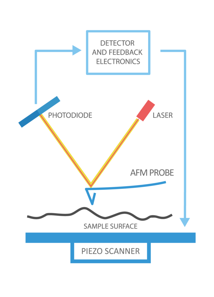
Schematic representation of AFM
Image source: https://www.nanoandmore.com/what-is-atomic-force-microscopy
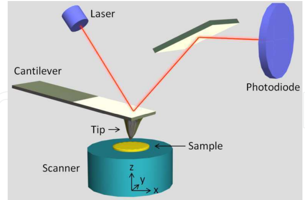
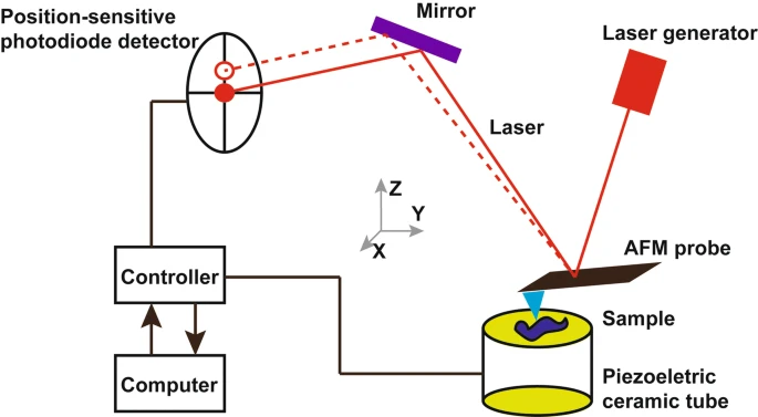
The materials Si3N4 and Si are frequently used to fabricate the extended ‘tip’ at the cantilever’s end. The nanoscope AFM has a reflecting cantilever at its base, where the tip is attached. In this case, a diode laser is trained on a reflecting cantilever. The laser beam is deflected off the cantilever into a photodiode as the tip moves up and down on the surface of the sample, following its shape. The light intensity differential between the top and lower photodetectors is converted to a voltage by the photodetector. This constant force or constant height mode is made possible by the photodiode’s feedback. A piezotransducer is used to measure vertical displacement in the constant force mode. With the AFM set to constant height mode, the force of deflection on the sample can be recorded.
Wafers of up to 200 millimeters in diameter can be analyzed using certain types of AFMs. These devices’ principal function is to quantitatively quantify surface roughness on a wide variety of samples with a resolution of 5 nm laterally and 0.01 nm vertically, respectively. In some types of atomic force microscopes (AFMs), the sample is moved underneath the cantilever, while in others, the cantilever is moved on top of the sample. These two techniques can be utilized to measure the height of the sample at its specific location. A three-dimensional topographical map of the surface can be generated by plotting the local sample height as a function of the horizontal tip location. Because atomic force microscopy (AFM imaging) is a three-dimensional imaging technique, the idea of resolution in AFM imaging is distinct from that of radiation-based microscopy techniques. The resolution of the pictures produced by techniques based on optical methods is restricted by diffraction, but the resolution produced by scanning probe methods is regulated by the geometry of the probe and the sample. Because the diameter of a DNA molecule in its B form is known to be 2.0 nm, the width of a DNA molecule is typically used in a very general sense as a measure of resolution. In the case of AFM imaging, a resolution of 3.0 nanometers based on the DNA in propanol is among the best results. Unfortunately, this definition of resolution can sometimes lead to misunderstandings due to the sample height’s obvious impact on the value being discussed.
Atomic force microscopy principle
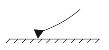
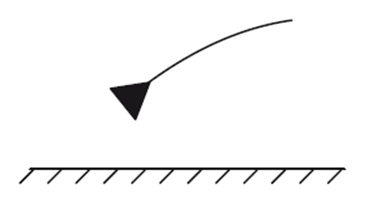
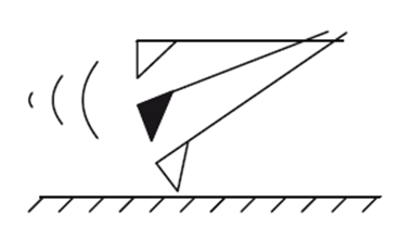
The sharp tip of an atomic force microscope is attached to a flexible cantilever. When the tip is scanned very close to the surface of the sample, i.e. within a few of the surface of the sample, forces between the atoms on the tip and those on the sample are made. These forces can be either repelling or attracting. The force that pushes or pulls makes the cantilever move. How much the tip moves varies on the distance “d” between the tip and the sample. Atoms on the tip of the AFM will contact with atoms on the surfaces.
Schematic representation of the principle of AFM
Image source: https://pdfs.semanticscholar.org/a54a/84b7a501bf58e7ae029a84c5c71d0f662324.pdf
The displacement (x) of the cantilever from its starting position is given by
X= – f/k
Where k= spring constant of the cantilever and f = restoring force
Optical lever or beam-bounce detection is the most common method used to track deflection. Reflected light from a laser diode at the cantilever’s back is detected by a photodiode that is sensitive to changes in position. Once the laser beam is focused on the positive-sensitive photodiode (detector), the corresponding cantilever deflection can be determined. Coating the cantilever’s back with gold or another metal improves its ability to reflect the laser beam, allowing more of it to reach the detectors.
Modes of operation of Atomic force microscopy
Since the development of the AFM technique, numerous AFM modes have emerged for specific purposes. Contact mode, non-contact mode, and tapping mode are three frequently employed strategies that are explained here.
Contact mode
In contact mode, the most typical setup is one in which the tip is brought into very close proximity to the surface that is being scanned. On the tip, a force of roughly 10–9 N in the opposite direction is applied. The tip is brought into contact with the surface of the sample by a piezoelectric positioning element. In contact mode AFM, the amount of tip deflection is measured and compared to a target value. When the measured value does not match the desired value, a voltage is supplied to the piezo to modify the vertical position of the sample relative to the tip in order to restore the desired value of deflection. This is done so that the measured value matches the desired value. As a result, the height and depth of features on the surface of the sample can be measured by the voltage that is delivered to the piezo. There are a few instruments that can work in UHV, however, the vast majority of them can either operate in liquids or in an ambient atmosphere.
When investigating biological specimens, for instance, or the influence of adsorbed layers, the effect of the impressed force on the surface might lead to limits. These constraints can be caused by the action of the impressed force. By lowering the tracking force that the probe exerts on the sample, it is possible to alleviate some of the effects of this. A layer of adsorbed gases, typically composed of water vapor and nitrogen, covers sample surfaces while they are in circumstances that are considered to be ambient. The thickness of this layer ranges from 10 to 30 monolayers. Surface tension causes a pulling force that brings the tip closer to the surface of the sample when it comes into contact with the contaminated layer. The size of the force is determined by the specific shape of the probe, however, it is normally on the order of 100 nano-Newtons. By carrying out the experiment with the probe and ensuring that all or part of the sample is completely submerged in liquid, it is possible to counteract the meniscus force as well as other attractive forces.
Operating the atomic force microscope (AFM) with the sample and cantilever immersed in a fluid has a number of advantages. These advantages include the elimination of capillary forces, the reduction of van der Waals forces, and the ability to study liquid–solid interfaces. However, there is a possibility that there will be issues, such as liquid leakage or damaged samples, etc. The combination of all of these phenomena might make imaging difficult or even result in the cantilever probe breaking. Imaging these types of specimens is best accomplished through the use of a non-contact mode.
Non-contact mode
The non-contact mode of the AFM study has resulted in a new era in imaging because it enables far greater diversity in imaging surfaces without the risk of causing harm to surface features or the tip. This has opened up a new era in imaging. In this mode, the cantilever tip is raised to a height that is approximately 5–15 nm above the surface of the sample.
The topographic image of the surface is obtained by using the van der Waals forces that are acting between the tip and the sample as the basis for the calculation. However, the van der Waals forces involved in this mode are significantly less powerful than those involved in the contact mode. In order to solve this issue, a slight oscillation is applied to the tip, and then the change in amplitude, phase, and frequency of the oscillating tip is monitored. This allows the small forces that are exerted between the tip and the sample surface to be identified. It is important to detect force gradients from van der Waals forces in order to achieve the best resolution possible. These forces may reach only one nanometer inward from the surface of the sample. However, because the fluid contaminant layer is significantly thicker than the van der Waals force gradient, the oscillating probe has the potential to become trapped in the fluid layer. This makes imaging with the non-contact tip extremely challenging.
Tapping mode
The tapping mode is a prospective technique that allows for high-resolution topographic imaging of sample surfaces. It helps overcome some of the limitations of the contact and non-contact modes of imaging, which were previously limitations of those modes. The tapping mode solves the issues that are caused by friction, adhesion, electrostatic forces, and other challenges that are present in conventional AFM scanning methods. During this mode, the tip is oscillated using a piezoelectric crystal at a frequency that is either identical to or very close to its resonance frequency.
When the tip is not in touch with the surface, the piezo causes it to oscillate at a high frequency with a high amplitude (more than 20 nm). The tip is slowly lowered till it comes into contact with the surface in such a way that it only lightly contacts the surface. The oscillating nature of the tip leads the tip to briefly come into contact with the surface before lifting off of it. The cantilever has a frequency that ranges from around 50,000 to 500,000 cycles per second when it is tapping the surface. Because of the transfer of energy that occurs when the oscillating tip makes contact with the surface, the oscillation of the tip is dampened. The fluctuation in the amplitude of the oscillation is what is used to detect the surface characteristics. During the tapping mode, a feedback loop keeps the cantilever’s oscillation amplitude stable so that it may be accurately measured. When the tip of the oscillator moves over a surface depression or protrusion, the amplitude of the oscillation either decreases or increases, depending on the type of feature. After then, the digital feedback loop will make the necessary adjustments to the tip–sample separation in order to keep the amplitude and force on the sample constant.
When the tip makes contact with the surface, the high frequency (between 50k and 500 kHz) causes the surface to become rigid (viscoelastic), which results in a significant decrease in the adhesion force between the tip and the sample. During the scanning process, the tip will not stick to the surface and cause any damage because the tapping mode prevents this from happening. When using the tapping mode, as opposed to the other two modes, the tip that is in contact with the surface has an oscillation amplitude that is sufficient enough to overcome the adhesion forces between the tip and the sample. Since the force is being applied vertically, there is virtually no shear force being exerted, and as a result, the surface material is not being pulled in a lateral direction. Reproducible sample measurements are made possible thanks to the tapping mode technique’s vast, linear operating range, which is yet another of the method’s advantages.
Imaging in a fluid medium has a tendency to attenuate the tip’s resonance frequency when tapping mode operation is being performed. When the cantilever makes contact with the surface, the amplitude of the cantilever’s oscillation experiences a dramatic reduction. The frequency of oscillation in fluids is typically around 5000. up to 40,000 cycles in a single second. When compared to the tapping mode in air, where the cantilever might be anywhere between 1 and 100 N/m, the spring constant is typically measured in units of 0.1 N/m. Because of this, imaging in fluids is made more accurate.
Instrumentation of Atomic Force Microscopy
The instrumentation of AFM is presented below:
Instrumentation of AFM
Image source: https://jnanobiotechnology.biomedcentral.com/articles/10.1186/s12951-018-0428-0
Some of the major parts of AFM are:
- Scanning probe: To scan a sample’s surface, this extremely fine and sharp tip is attached to the end of a cantilever. The probe is typically only a few nanometers in size and composed of a hard, robust substance like diamond or silicon.
- Cantilever: This is a thin and flexible beam that gives the probe stability and mobility. Lightweight materials like silicon or silicon nitride are used to create the cantilever, which is only a few micrometers in length and a few hundred nanometers in thickness.
- Scanning stage: This setup provides a stable base for the sample while allowing for precise positioning in relation to the probe. Typically, precision motors or piezoelectric actuators are used to move the stage in extremely fine increments, and the stage itself is made of lightweight, rigid material like aluminum.
- Detection system: This apparatus monitors not only the probe’s position relative to the sample but also the forces exerted by the sample on the probe. Optical, capacitive, and piezoresistive techniques are only a few of the many available for detecting these numbers.
- Control and acquisition system: This computer controls the probe and sample and analyses detection system data. A computer, software, keyboard, mouse, and display screen constitute the control and data acquisition system.
- Feedback loop control: A laser deflector controls force interactions and tip positions, generating a feedback loop for precise manipulation. The feedback loop uses the laser’s position on the photodetector to track and measure the sample’s surface while the cantilever’s tip interacts with it.
- Detection: The atomic force microscope has a laser beam deflector. The reflecting AFM lever back reflects laser to sensitive detector. Silicon compound tips are 10nm.
- Force measurement: It is the force interactions between the probe and sample that make the AFM work and produce usable images. Knowing the rigidity of the cantilever allows one to measure the forces by calculating the deflection lever. The formula for this calculation is given by Hooke’s law and looks like this: Where F is the force, k is the lever’s stiffness, and z is the lever’s degree of bending, F= -kz.
Comparison of Atomic Force Microscopy (AFM) and other imaging techniques
AFM versus STM
The relationship between AFM and the precursor, scanning tunneling microscopy, is interesting. Because the tunneling current depends exponentially on distance, STM can sometimes provide higher resolution than AFM. STM can only be used to study conducting samples, however, AFM can be used on both conducting and non-conducting samples. When compared to STM, AFM’s adaptability is much greater. While in STM the tip-to-substrate distance is tied to the voltage, in AFM the two can be adjusted independently in AFM.
AFM versus SEM
Topographic contrast, direct height measurements, and clear inspection of surface features (no coating required) are some of AFM’s advantages over the scanning electron microscope (SEM). Surface topography can be measured using one of these methods. Other physical surface properties can be measured with either type of microscope. SEM is favored for analyzing surfaces’ chemical composition, while AFM is favored for analyzing their mechanical qualities.
AFM versus TEM
Three-dimensional AFM images are produced without costly sample preparation and give significantly more detailed information than two-dimensional profiles accessible from cross-sectioned samples, both of which are limitations of the transmission electron microscope.
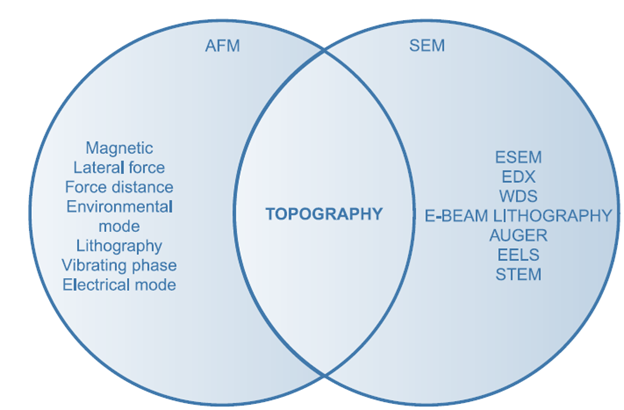
The atomic force microscope (AFM) has served as an inspiration for a wide variety of different scanning probe techniques. The atomic force microscope (AFM) was initially developed largely for the purpose of understanding the topography of surfaces in its earlier stages of development. In recent years, the tip has been modified to assess electric and magnetic properties, as well as chemical reactions and concentrations. The scanning electron microscope (SEM) and transmission electron microscope (TEM) are two of the most common comparisons made with the atomic force microscope (AFM). Because only minimal sample preparation is necessary when using an AFM, it is generally simpler to learn how to use an AFM than it is to learn how to use a SEM. When performing an AFM scan, the quality of the image obtained is heavily dependent on the tip that is used.
Nanoparticles with sizes ranging from a few nanometers to a few microns are not a problem for the AFM to visualize. It is feasible to measure both the size of individual nanoparticles and the parameter distribution of an ensemble of nanoparticles. One can measure the size of individual nanoparticles. A number of parameters, including particle size, It is simple to obtain measurements for volume, circumference, and surface area. The development of methods for dispersing nanoparticles over a surface is one of the primary obstacles that must be overcome in order to accurately measure nanoparticles. Visualization in all three dimensions is possible with the AFM. Resolution in the vertical or z-axis is restricted by the vibration environment of the instrument, whilst resolution in the horizontal or xy-axis is limited by the diameter of the tip that is used for scanning. Both of these factors contribute to the overall resolution of the instrument. AFM instruments typically have vertical resolutions that are lower than 0.1 nm, while their xy-resolutions are typically somewhere about 1 nm.
It is possible to generate quantitative information from individual nanoparticles and between groups of nanoparticles through the use of software-based image processing of AFM data. It is possible to measure not only the size information of individual particles (such as their length, width, and height), but also other physical qualities, such as their morphology and surface roughness. It is also possible to measure statistics regarding a group of particles, such as the distribution of particle size.
Advantages of Atomic Force Microscopy
- High resolution
- Non-destructive imaging
- Versatility
- Three-dimensional imaging
- Nanoscale manipulation
- Easy sample preparation
- More reliability
- More accurate surface Study
Applications of Atomic Force Microscopy
Due to its adaptability to room temperature and a wide variety of environments, AFM has many potential uses as:
- It has a wide range of potential applications and can be used to study a wide variety of materials and organisms, including semiconductors, polymers, nanoparticles, biotechnology, and cells.
- Most frequently, AFM is used in morphological research to acquire information about the sample’s topography.
- Since the material is often in solution, AFM can also provide insight into its dispersibility and particle homogeneity within a given dispersion.
- It’s also useful to understand a lot about the particles being researched, like their size, surface area, electrical properties, and chemical composition.
- Investigating the physical and chemical characteristics of protein assemblies and complexes like microtubules.
Suggested video:
References
- https://pdfs.semanticscholar.org/a54a/84b7a501bf58e7ae029a84c5c71d0f662324.pdf.
- https://jnanobiotechnology.biomedcentral.com/articles/10.1186/s12951-018-0428-0.
- https://doi.org/10.1021/acs.chemrev.0c00617.
- https://www.nanoscience.com/techniques/atomic-force-microscopy/.
- http://balintszabo.web.elte.hu/SzerkVizsgBiofiz/AFM.pdf.
- https://www.researchgate.net/publication/322294428_Atomic_Force_Microscopy.
- https://asdlib.org/onlineArticles/ecourseware/Bullen/SPMModule_BasicTheoryAFM.pdf.
- https://www.unige.ch/sciences/chifi/wiki/lib/exe/fetch.php?media=sugi:peter_eaton_paul_west_atomic_force_microscopy_bookfi_.pdf.